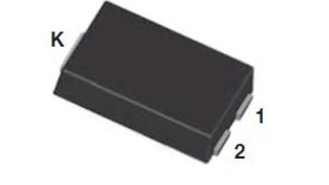
Principle of Schottky Diode
Date:2025-05-21 Categories:Product knowledge Hits:536 From:Guangdong Youfeng Microelectronics Co., Ltd
1. Introduction
Schottky Diode, also known as Schottky barrier diodes (SBDs), are semiconductor devices renowned for their unique electrical properties, especially their fast switching speed and low forward voltage drop. These characteristics make them indispensable in modern electronics, from power supplies to high-frequency circuits. Understanding the principle of Schottky diodes requires a deep dive into the interaction between metals and semiconductors, as well as the behavior of charge carriers at their interface.
A
Schottky Diode is fundamentally constructed from a junction between a metal and a lightly doped n-type semiconductor. Typically, metals like platinum, tungsten, or molybdenum are used, while n-type semiconductors such as silicon (Si) or gallium arsenide (GaAs) serve as the semiconductor base. In the n-type semiconductor, electrons are the majority carriers, while holes (absence of electrons) are the minority carriers.
The key to the
Schottky Diode’s operation lies in the formation of a Schottky barrier at the metal-semiconductor interface. When the metal and n-type semiconductor are brought into contact, a depletion region forms near the interface. Unlike in a traditional p-n junction diode where the depletion region results from the diffusion of holes and electrons across the junction, the Schottky barrier depletion region is created due to the difference in work functions between the metal and the semiconductor.

Previous:
Classification, Structure, and Principle of MOSFET
Next:
Renesas tunable antenna varactor diodes for One-Seg broadcasting applications 1
