
Date:2025-09-01 Categories:Product knowledge Hits:386 From:Guangdong Youfeng Microelectronics Co., Ltd
Safe Operating Area
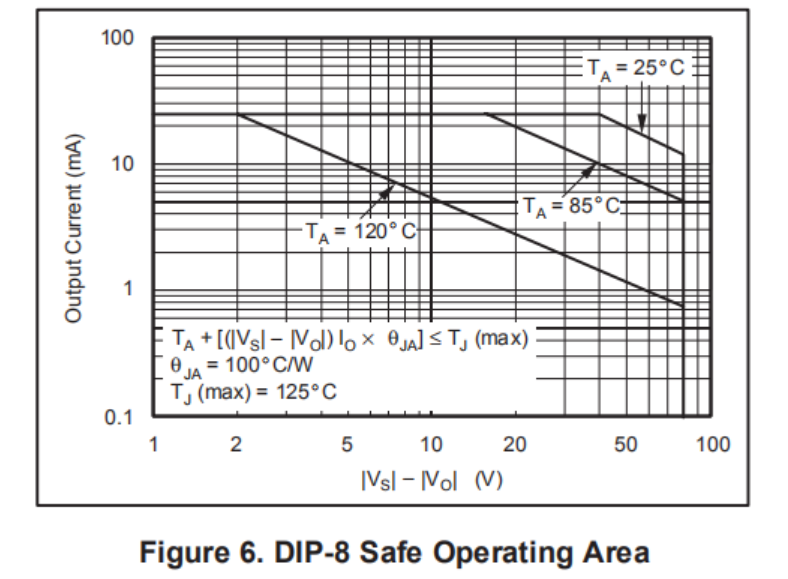
The stress on the output transistor is determined by the output current and the output voltage VS-VO of the conductive output transistor. The power consumed by the output transistor is equal to the product of the output current and the voltage passing through the conductive transistor, VS−VO。 The safe operating zone (SOA curve, Figures 6 to 10) illustrates the allowable range of voltage and current. The curve shown represents a device without heat dissipation fins soldered onto a printed circuit board (PCB). Increasing the printed circuit trace area or using heat sinks (TO-99 package) can significantly reduce thermal resistance, thereby increasing output current at a given output voltage (see Figure 11, Figure 12, and heat sink section).transistor
As VS-VO increases, the safe output current decreases. Output short circuit is a very demanding situation for SOA. A ground short circuit forces the entire power supply voltage (V+or V -) to pass through the conductive transistor and generate a typical output current of 25 milliamps. For a ± 40V power supply, this will result in an internal loss of 1W.
This exceeds the maximum rated value and is not recommended for use. If it is unavoidable to operate in this area, a radiator is required. To further understand SOA, please refer to Application Bulletin SBOA022.transistor
Previous: Classification, Structure, and Principle of MOSFET
Next: Renesas tunable antenna varactor diodes for One-Seg broadcasting applications 1